Introduction
Welcome to developing on FPGAs.
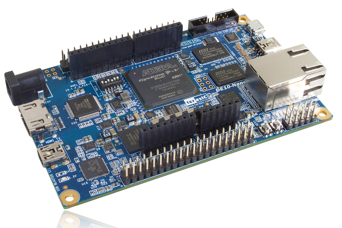
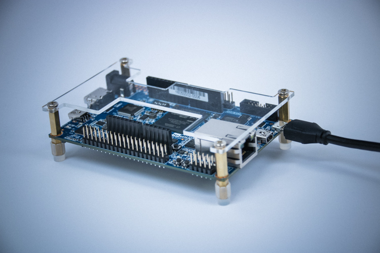
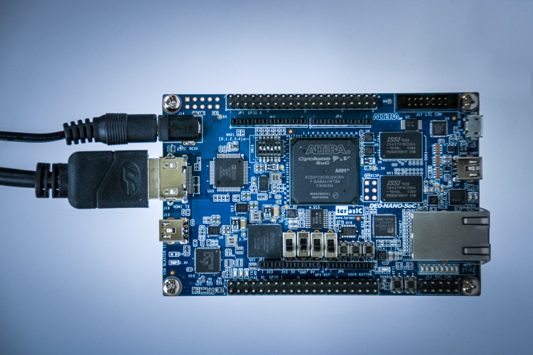
The Terasic DE10-Nano development board, based on an Intel® SoC FPGA, provides a reconfigurable hardware design platform for makers, IoT developers and educators. Featuring two GPIO expansion headers, an Arduino* header, high-speed DDR3 memory, an HDMI* port and ethernet networking, the board provides a robust and feature rich platform to create many exciting IoT applications.
Developers and makers are invited to discover the performance of a low-power embedded processor integrated with the flexibility of programmable logic. Divided into two distinct parts, the Intel® Cyclone® FPGA SoC device is made of a hard processor system (HPS) and a Field Programmable Gate Array (FPGA). While the HPS is a general purpose processor (based on a dual-core ARM Cortex-A9* processor), the FPGA is a parallel processing engine on which you can create custom hardware to accelerate fixed function algorithms or for extending the I/O capabilities of the device.
Follow along with the chapters (pages) of this Get Started Guide to get your board up and running. We walk you through the assembly and set up, configuring the FPGA and then connecting your host PC to the board. Then we take you to the webpages hosted by board where you can play with the interactive web demos. After familiarizing yourself with the demos, head to the Projects section and check out some of the tutorials where you can learn more about the GPIO LED framework, details of the Fast Fourier Transform (FFT), and debugging applications with the ARM* DS-5 debugger. For more ambitious developers, head straight to My First FPGA section or check out the On-board Accelerometer Tutorial section (be careful when you shake the board.).
Whether you are an FPGA developer, software developer, maker, seasoned IoT developer, coding newbie, or just curious about FPGAs, we hope your experience with the Terasic DE10-Nano kit is both informative and fun.
Let's get started.
Terasic DE10-Nano Kit Contents
Before you begin, inventory and verify the kit contents.
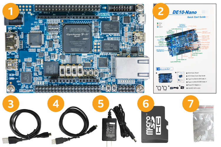
Contents
- Terasic DE10-Nano Board
- Quick Start Guide (paper pamphlet)
- Type A to Micro-B USB Cable
- For USB* OTG port
- Type A to Mini-B USB Cable
- Two functions: UART and USB Blaster
- 5V (2A) DC power supply
- microSD* card
- Bag of four rubber (silicon) foot stands
Host System Requirements
- Compatible Operating Systems: Linux or Windows®
- USB 2.0 Port (for USB OTG Cable)
Note The Intel® Quartus® Prime Software Suite supports Windows* 7, 8.1, and Windows® 10.
Terasic DE10-Nano Assembly and Setup
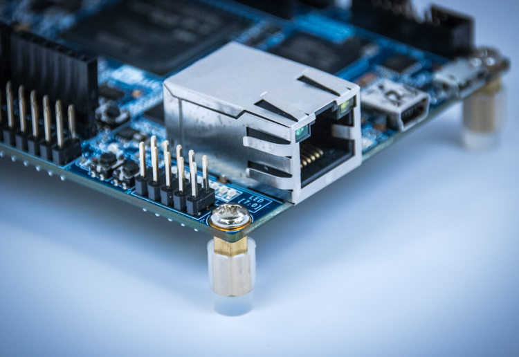
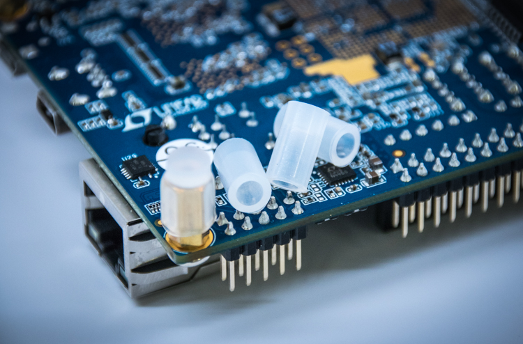
- For board stability, attach the silicon (rubber) feet to the copper standoffs (underside of board).
- Insert the microSD* card.
- Verify the switch settings.
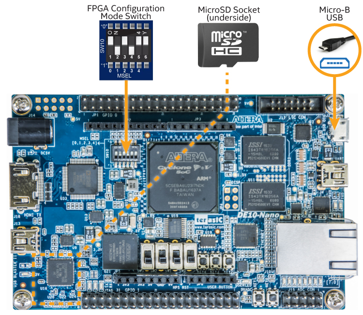
Note If the switch settings are not as shown, you can use a wooden toothpick to change the 6 pin DIP switch (SW10 on the Terasic DE10-Nano board) for the FPGA Configuration Mode Switch settings.
Once the board is powered on, the mode select (MSEL) pins (implemented as the 6 pin DIP switch on the board) determine how the FPGA will be configured—from EPCS or HPS (hard processor system). Here, the MSEL control pins are set to configure the FPGA by the processor under software control.
Powering on the board
To power on the board connect the power adapter and plug in the power cable (DC 5V) into a wall outlet. Now, watch for the onboard LEDs to light up. You should see the following boot sequence (of flashing LEDs):
Note The board does not have a dedicated "power button" and powering on the board here means inserting the power plug into a wall outlet.
Boot sequence
- Blue LED: 3.3 V power LED lights up.
- Amber LED: Indicates that the FPGA has been configured.
- Green “Heartbeat” LED: A pulsing or 'heartbeat' LED indicates that the Linux* OS has been loaded.
- Green user LEDs [7:0]: Counts down from LSB to MSB. Indicates that the device tree overlay has been loaded. What that means is that Linux now knows about the LEDs (so why not blink them.).
If you've made it this far, it means everything is working. Now that the FPGA has been successfully configured, you're now ready to connect your host PC to the board. The board acts as a webserver and serves up (or hosts) webpages containing details about the board, interactive demo applications, and learning resources for developers.
Let's get connected to the board and play with the web demos.
Connect to the Terasic DE10-Nano
You have two options to connect your host system (e.g., laptop) to the board:
- Ethernet over USB
- Serial Connection
Ethernet over USB uses the USB* OTG port on the board and the the micro-b USB cable that comes in the Terasic DE10-Nano kit. A serial connection uses the board's UART port (located between the Ethernet port and the USB OTG port on the board) and the mini-b USB cable in the kit.
This section covers connecting to the board through Ethernet over USB. For instructions on how to set up a serial connection to the Terasic DE10-Nano, check out Setting up a Serial Terminal.
Objectives
First, we'll connect to the board (through Ethernet over USB) in order to navigate to the website hosted by the Terasic DE10-Nano board and test out some fun demo applications. Then, we connect to the board's desktop to take a deeper dive and explore some example applications (GPIO LEDS and FFT).
Extra There may be an accelerometer easter egg hiding on the board's desktop.
Navigate to the Website Hosted by the Board
Once the FPGA has been configured, you're ready to navigate to the web pages served up by the board. When you type the board's IP address (remember, the board acts or functions as a web server here) into a browser, you'll be taken to a website (hosted by the board) where you can interact with the hardware.
Using this web site you'll discover additional details about the board, play with some fun demo applications (blink the onboard LEDs.), learn about SoC FPGA software flow, and install tools needed for development using Intel® SoC FPGA devices.
Let's get connected to the board.
Ethernet over USB
The Terasic DE10-Nano can access the internet through your computer (host system) via the USB micro-B cable. It's Ethernet over USB* OTG.
- Use the micro-b USB cable to connect the board (USB OTG port) and your host system (Type-A end of the cable connects into a standard USB port on your computer).
- If you've unplugged the power cable, plug it back into the board.
- Open file explorer and navigate to the device “DE10-Nano”. The board is represented as a mass storage device.
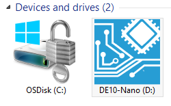
- Right click and “Open” the device to view the contents.
- Here’s what’s on the SD card:
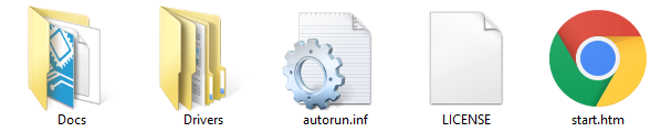
- For Windows* PC users, you'll need to install a driver to enable Ethernet over USB before connecting to the board. Follow the instructions in the start.htm page to install the appropriate driver to enable Ethernet over USB.

- Open your web browser (Google Chrome* or Firefox* recommended), and type the IP address 192.168.7.1 into the URL pane.
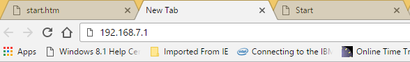
You've now arrived at the webpage hosted by the Terasic DE10-Nano board. Navigate to the Play tab and test out the demo applications.
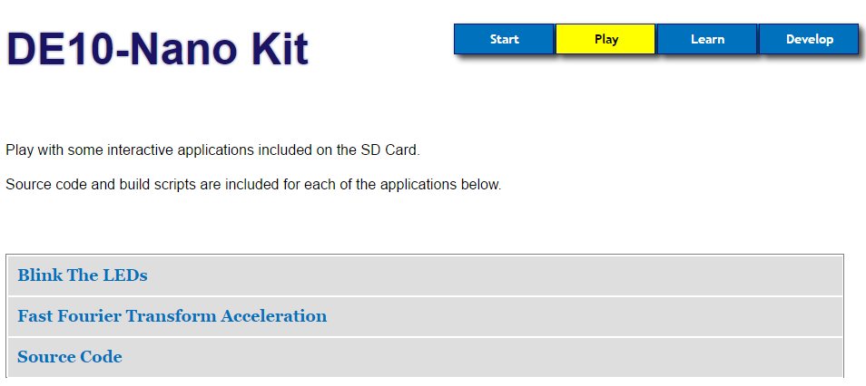
You can blink the onboard LEDs and learn more about the Fast Fourier Transform (FFT) Acceleration.
There are two sets of LEDs connected to the SoC device. One LED is connected to a GPIO pin of the ARM processor, and eight others are connected to the FPGA I/O pins. This design controls the LEDs connected to the FPGA.
Once your familiar with those applications, you can head on over to Explore GPIO LEDs Example Application, Explore Fast Fourier Transform (FFT) Example Application, and FPGA Accelerometer Tutorial to learn more about how to build these applications (run some scripts and create an executable file).
But first, we need to connect to the board's desktop.
Connect to the Board's Desktop
When you connect to the board, you'll have access to the tools and design examples on the board so you can build some of the demo applications you played with (when you navigated to the Play tab after typing the board's IP address into a web browser).
There are three methods you can choose from to connect to the board's desktop:
- Virtual Network Computing (VNC)
- Secure Shell (SSH)
- HDMI*
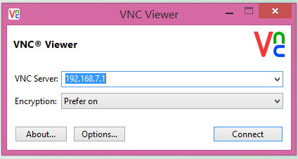
VNC
- Launch VNC Viewer
- Connect to the VNC Server (board's IP address): 192.168.7.1
Download VNC Viewer
SSH
You can connect via SSH from either a terminal (shell) or using the PuTTY software.
- Terminal
- From a terminal (console) window type: ssh root@192.168.7.1
- PuTTY
- Launch PuTTY
- Type board's IP address in the host name field: 192.168.7.1
- Select 'SSH' for Connection Type
- Click Open
- At the login prompt type: root
HDMI*
To connect via the HDMI port, connect an HDMI cable to a HDMI compatible monitor. Connect the HDMI cable to the monitor first then power on the board. You will also want to install the Synergy software for mouse and keyboard or you can use a wireless mouse and keyboard (you'll need an adapter for the usb dongle).
- Plug in the HDMI cable first. Make sure the monitor is powered up too.
- Next plug in the power to the board.
Note The Terasic DE10-Nano board needs to be connected to a powered up monitor via HDMI prior to starting (applying power) the board.
Once you've successfully connected to the board, head on over to the Explore the GPIO Example Application article to learn more about how to interact with the LEDs registered under the GPIO framework.
We hope your experience with the Terasic DE10-Nano kit is fun and informative. And when you’re ready, head on over to the Develop page and tell us about your experience using the online survey (bottom of the page). Your feedback helps us to make the next release even better.
How to Set Up a Serial Terminal
This section provides steps to set up a serial terminal to communicate with your Terasic DE10-Nano* development board. You will need to set up a serial terminal to the board in order to set a static IP for the On-board Accelerometer Tutorial. A serial connection additionally gives you access to a wide range of functionality including:
- Connecting your board to a Wi-Fi* network
- Setting a password for your board
- Identifying your board's IP address
- Checking the version of the firmware on your board
- Updating the I/O and sensor libraries on your board to get access to the latest batch of supported sensors
To set up serial communication with your board, click on the appropriate link below:
For a quick list of useful commands for communicating with your board over a serial connection, see Common Commands for the Terasic DE10-Nano* board.
Setting Up a Serial Terminal on a System with Windows*
Follow along with the steps below to set up a serial connection to the Terasic DE10-Nano board.
Prerequisites
- You have already gone through the initial board assembly and setup. For steps to set up and assemble your Terasic DE10-Nano board, check out the Terasic DE10-Nano Assembly and Setup section.
- To set up a serial connection to the board, you'll need to download and install a client like Putty or TeraTerm.
- Install the FTDI D2XX driver to enable serial connection to the Terasic DE10-Nano via UART.
- USB cable (mini-b).
Steps
- Connect the board to your host system using the mini-b USB cable.
- Launch PuTTY.
- Configure the PuTTY menu.
- Log in and set password for serial terminal window.
Note If you are setting up a serial terminal for the accelerometer tutorial and you have the micro-b USB cable connected to the board and your host system, unplug it now. This is for Ethernet over USB. There are two different network interfaces on the Terasic DE10-Nano board: 1) Ethernet RJ45 as eth0 and 2) Ethernet over USB (RNDIS) as usb0. For the accelerometer exercise we use the eth0 interface.
Step 1: Connect the board to your host system using the mini-b USB cable.
The mini-b end connects to the UART port on the Terasic DE10-Nano board and the other end of the cable (type-A) is inserted into a standard USB port on your host system. Your board should also be powered on at this point. If not, apply power to the board.
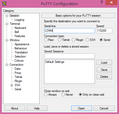
Step 2: Launch PuTTY

Step 3: Configure the PuTTY Menu
- Under Connection type, select Serial.
- For Serial line, enter the COM# for the board (e.g., COM5).
Note To identify the COM# for the Terasic DE10-Nano board, navigate to the Device Manager and look for an entry called Ports (COM & LPT) then expand that section and find the USB Serial Port entry. The COM# is displayed next to the USB Serial Port entry in parentheses. If you don't see the USB Serial Port entry, you may need to select the View tab in Device Manager and check "Show hidden devices". Also, make sure the FTDI D2XX driver installed properly. - In the Speed field, type 115200.
- Click Open.
Step 4: Log In and Set Password for Serial Terminal Window
- A blank terminal window should pop up. Press the Enter key twice for a login prompt.
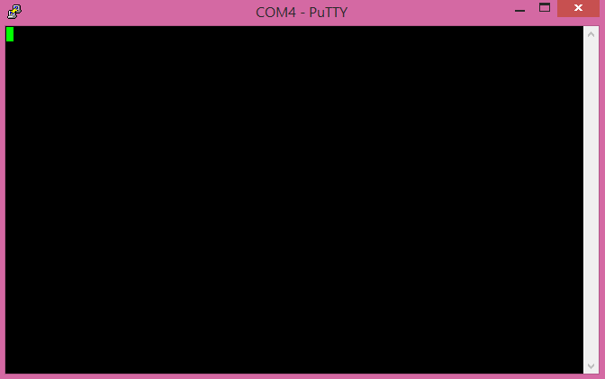
- At the login prompt, type root and then hit Enter.
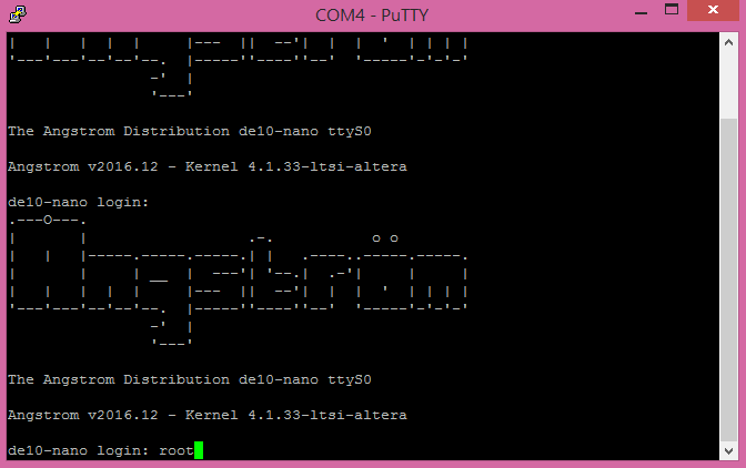
- When prompted for a password you can press Enter. However, if you want to set a password, use the passwd command to create a password (your choice).
- You should now see a terminal prompt root@de10-nano:~#.
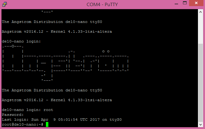
Congratulations. You've established a serial connection to the Terasic DE10-Nano board. Through the serial connection, you can interact with the board by entering common Linux commands. For a summary of useful commands for the Terasic DE10-Nano board, see Common Commands for the Terasic DE10-Nano board
Common Commands
This section contains common commands you can enter to communicate with the Terasic DE10-Nano board through serial communication.
| Description | Command |
|---|---|
| Check the board's firmware version | cat /etc/version |
| Display the board's IP information | ifconfig |
| Change the board's login password | passwd |
| Display a help message with additional common commands | help |
Terasic DE10-Nano Tutorial Projects
This section contains tutorial projects for the Terasic DE10-Nano board.
Check out the GPIO Example Application section to learn more about the 8 green user LEDs registered under the general-purpose input/output (GPIO) framework. Get familiar with the source code used to execute the Fast Fourier Transform (FFT) in the Explore FFT Example Application section. Or head on over to the On-board Accelerometer Tutorial section to plot and capture accelerometer data from the board's built-in accelerometer. Get introduced to the ARM* DS-5* debugger in the Debug 'Hello World' Application section. And don't forget to check out the My First FPGA tutorial where you learn to program your first FPGA device (blink an LED.).
- Explore GPIO Example Application
- Explore FFT Example Application
- On-board Accelerometer Tutorial
- Debug 'Hello World'
- My First FPGA
Explore GPIO Example Application
Learn about the Terasic* DE10-Nano board's digital I/O: User LEDs, slide switches and User push button.
If you've already visited the Play page of the website served by the board, then you've probably interacted with the board's user LEDs. The Blink the LEDs example on that page provides a simple web interface to turn either ON/OFF or blink the LEDs. You may be curious to learn what's happening behind the scenes of the demo application and we explore that in this tutorial where you learn to interact with the board's I/O:
- 8 green user LEDs
- 4 slide switches
- User push button
Check out the full tutorial.
Explore FFT Example Application
In this example application, you'll learn more about the source code used to execute the Fast Fourier Transform for both the FPGA and HPS (ARM* processor).
There's nothing to play with (no LEDs to blink) but you'll get a behind the scenes looks at the scripts and executables used to make the FFT web demo application.
Visit GitHub* for this project's code samples.
But before you VNC (you can also use the HDMI port or SSH) into the board and check out the FFT source code, let's quickly review the FFT demo application (it's purpose here and what the results mean). Plus a quick introduction to the Fast Fourier Transform.
FFT Web Demo Application
In the FFT demo application, you interacted with a Web interface (a simple GUI with buttons to test out sine, square, and triangle wave) to see the performance results—the time to calculate the FFT—of both the FPGA and HPS. Three sets of data (sample sizes) were used: 256, 4k and 1M samples. And the numbers (the table data) that came up measured the time (in microseconds) to process the Fast Fourier Transform. It was a race between the FPGA and ARM* processor (CPU) meant to demonstrate the parallel processing capabilities in the FPGA hardware (hint: FPGA wins here). Taking a closer look at the data, you'll see that the performance difference becomes obvious at a higher sample size (greater than 1M samples). Yes, there are twelve unique results that come up but that's only to be complete and thorough in capturing the various ways the data can processed. Not only can the data be processed by either the CPU or FPGA but the data source can come from two places: HPS (CPU plus some other stuff) or FPGA. The important thing is to focus on the time savings by the FPGA.
Fun Exercise
If you're feeling ambitious, collect and record at least 15 sets of data (you know, press the sine wave button 15 times) and plot the data in Excel. To make it easier, you can just record the data from one data source (pick FPGA or HPS but not both). And compare the performance (say from the FPGA data source) of the CPU versus the FPGA for 256, 4k, and 1M samples. You'll see that the difference (graphs are easier to read than data.) in performance becomes obvious at 1M samples. That is, at the higher sample size, we clearly see the hardware acceleration of a fixed function algorithm (here, the Fast Fourier Transform.). Can you figure out why that is? (Hint: it's got something to do with latency.)
What's a Fast Fourier Transform?
The Fast Fourier Transform is an alogrithm. It's used in signal processing and data analysis to measure every possible cycle (of a time series) and return the components of that cycle (e.g., amplitude). It takes a time-based data series and represents it in the frequency domain.
FFT Example Folder
Here we take a look at the FFT ReadMe file and run a script to install and execute the FFT example applications. This section is mainly to introduce you to the FFT source code so you can take a look under the hood of the FFT demo application. Again, nothing exciting happens here (as it did in the GPIO LED Example Application). No blinking of LEDs or anything tangible that comes up when you run any of the executables or scripts for this application. It's just code output (that's fun enough.)
Start a session with VNC Viewer and type the Terasic DE10-Nano board's IP address: 192.168.7.1
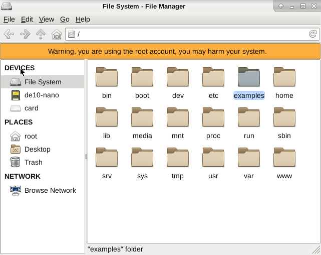
Navigate to the file system icon on the desktop and double click to open. Click on the examples folder.
Then open the folder FFT.
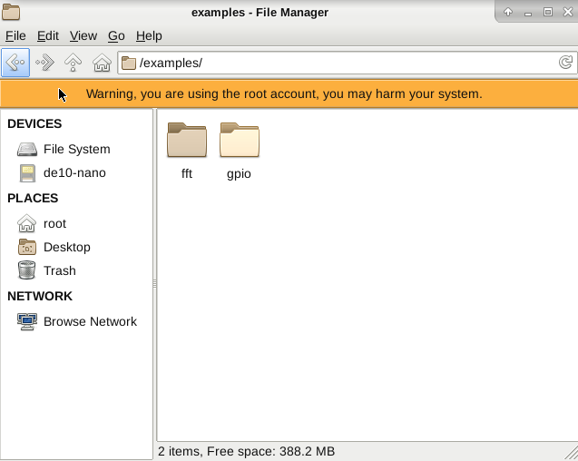
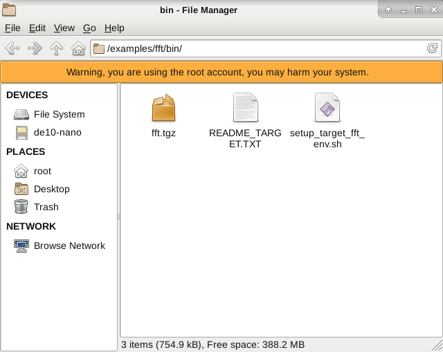
Click on the Bin folder.
This folder contains the ReadMe file and the main shell script you will run shortly.
Open a terminal emulator (console) window from the FFT folder. If you open up a terminal from the board's desktop, then cd into the fft directory.
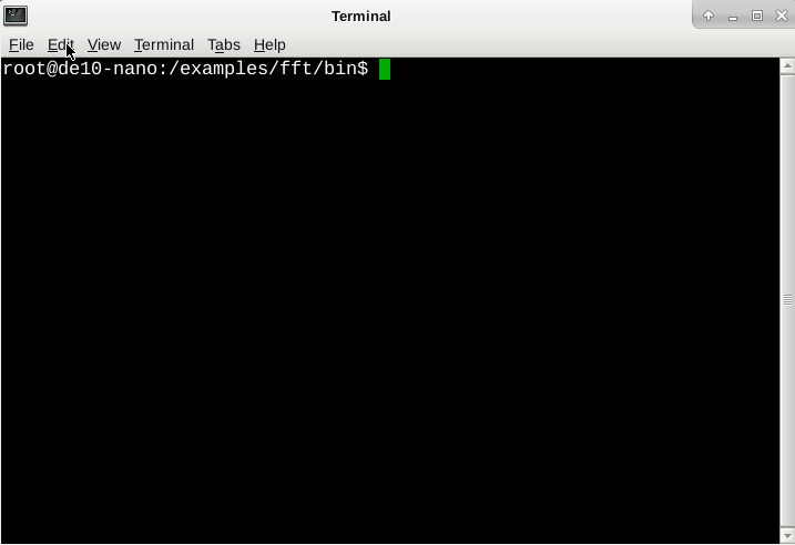
Run the following shell script in the terminal:
./setup_target_fft_env.sh
This script creates a directory /mnt/ram/fft/ which contains shell scripts and executable files. You may get an error if the directory already exists.
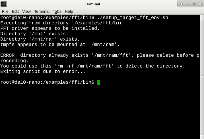
You can delete the directory by running the following command:
rm -rf /mnt/ram/fft
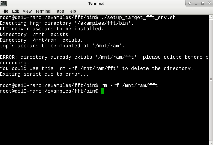
Run the shell script again:
./setup_target_fft_env.sh
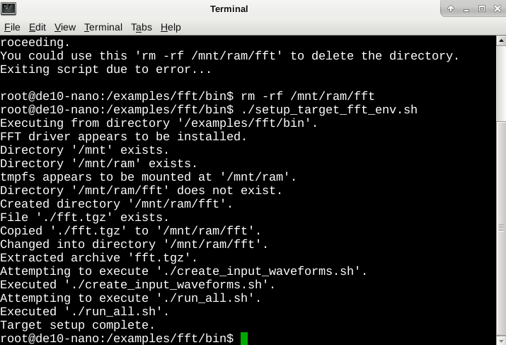
This target script will ensure the following:
- fft_driver is installed
- /mnt/ram has a 100MB tmpfs ram disk mounted
- extract the fft.tgz archive into /mnt/ram/fft
- runs the run_all.sh script
- run the create_input_waveforms.sh
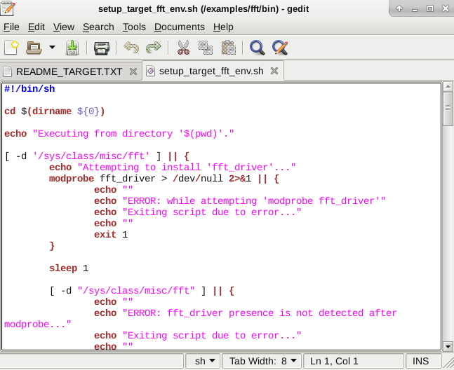
You can right click to open the .sh file and view the code to see more.
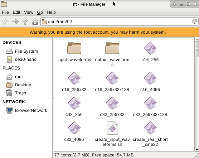
Now, about the scripts that are run: run_all.sh and create_input_waveforms.sh
- create_input_waveforms.sh <<< sine, triangle, square wave
- run_all.sh script <<< permutations of the demo applications (remember there were 12 unique results in the table from the FFT demo application)
The folder (/mnt/ram/fft directory) that was created contains the scripts and executable (also called applications) needed to run the FFT web demo.
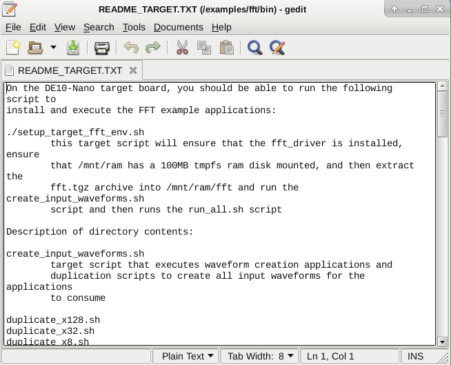
Open up the ReadMe file to learn about what each application or script (in the/mnt/ram/fft directory) does. Here, you can use Gedit to view the text file.
On-board Accelerometer Tutorial
Learn to capture and plot accelerometer data from the DE10-Nano board's built-in accelerometer.
Data from the built-in 3-axis accelerometer on the Terasic DE10-Nano (the ADXL345 from Analog Devices*) is measured on ALL 3 axes to show when the board is in motion. The raw output of the accelerometer is converted to g-force values by a sensor library and then sent to graphing software for data visualization and interpretation.
In this tutorial you will:
- Interface with the board's built-in digital accelerometer using an I2C* interface.
- Use Intel’s I/O and sensor libraries (MRAA and UPM) to get data from the accelerometer.
- Monitor and observe acceleration data for small vibration and movement along the x, y, z axes.
- Translate the acceleration data into +/- g-force values to demonstrate the motion of the Terasic DE10-Nano board.
- Show the accelerometer data using different open-source technologies:
-
- Express* (web server)
- Plotly* (graphing library)
- Websocket* (data stream).
Note Both Express.js and Plotly.js are non-restrictive MIT* licensed technologies.
Visit GitHub* for this project's code samples.
Debug 'Hello World'
Get introduced to the debug capabilities of the ARM* DS-5* debugger.
In this tutorial, you'll be introduced to the debug capabilities of the ARM* DS-5* debugger. In this tutorial, you'll create, compile and run the ‘Hello World’ example application on Linux* for the Terasic DE10-Nano Development Board. You’ll also learn how to import and compile a sample application, set up a remote system explorer, and create a debugger configuration to run and debug the application.
Learn more about the DS-5* from ARM*.
Prerequisites: Download and install the SoC Embedded Design Suite (SoC EDS) Standard Edition
The DS-5 Intel® SoC FPGA Edition is installed as a part of the embedded design suite you download above.
Note This section uses a host computer running Linux*, as can be seen from the screen shots and the issued commands. However, the scenario can also be run on a Windows* machine, although it is not usual for Linux development to be done on Windows.
Configuring Linux*
For this getting started scenario we need Linux to be running on the target board.
Eclipse* needs an account with a password to be able to connect to the target board. The root account does not have a password by default, so one needs to be set up. This can be achieved by running ‘passwd’ command from the serial console (on host system). Linux will then ask for the new password, then for password confirmation, then it will update.
Note Eclipse is part of the SoC EDS.
Import Sample Application
- Start Eclipse from Embedded Command Shell.
- In Eclipse, select File > New Project > C Project. The C Project dialog box displays.
- In the C Project dialog box, select Project Name to be “HelloWorldLinux”. Also select the Executable to be “Hello World Ansi C Project” and the Toolchain to be “GCC 4.x[arm-linux-gnueabihf]”.
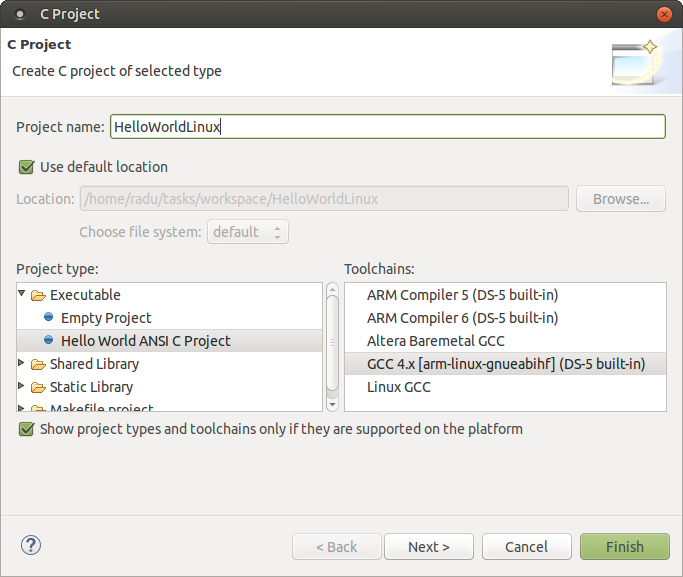
- Click Finish. The project is imported. The project files are displayed in the Project Explorer panel.
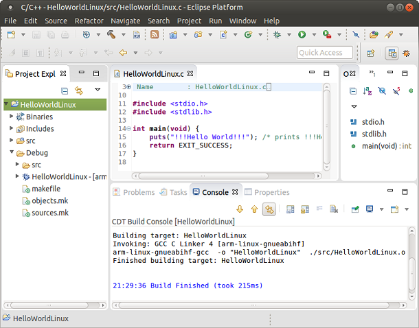
Compile Sample Application
- To compile the application, select the project in Project Explorer.
- Select Project > Build Project.
- The project compiles and the Project Explorer shows the newly created hello executable file as shown in the figure below. The Console dialog box shows the commands and responses that were executed.
Set up Remote System Explorer
The ARM DS-5 Altera Edition can run and debug programs directly on the target with the help of the Remote System Explorer (RSE). It has all the regular features of a debugger that include: load application, run application, step-by-step execution, view variables and registers, and evaluate expressions. Before this feature can be used, the RSE needs to be configured to connect to the target board running Linux.
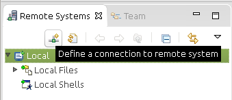
- In your Eclipse workspace, select Window > Open Perspective > Other. This will open the Open Perspective dialog box.
- In the Open Perspective dialog box, click the Remote System Explorer and click OK.
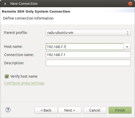
- In the Remote System Explorer view, right click Local and select New > Connection …. This will open the New Connection wizard. Note that Clicking the + icon achieves the same result.
- In the first page of the New Connection wizard, named Remote System Type view, select SSH only and click Next.

- Enter the IP address of the board in the Host Name field. Click Finish to create the connection.
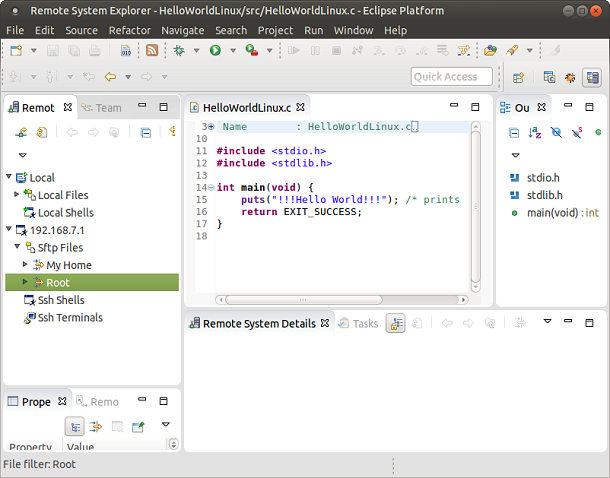
- In the Remote Systems panel, click the Target IP > Sftp Files > Root. This opens a dialog box to enter the username and password.
- Assign root to User ID and assign the password you selected in the “Configuring Linux” Section to Password. Check the Save User ID and Save password check boxes. Click OK.
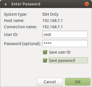
- Eclipse asks for confirmation of authenticity of the board. Click Yes.
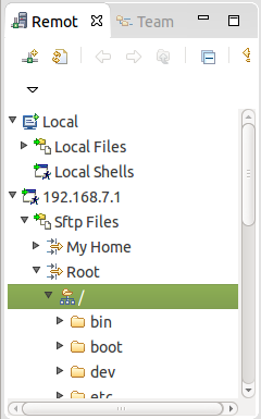
- Remote System Explorer shows the files on the board on the left panel.
Debug Sample Application
At this stage, we have a compiled Linux application and a properly configured Remote Systems Connection. This section shows how to create a Debugger Configuration and use it to run and debug the application.
- Select Run > Debug Configurations… to open the Debug Configurations dialog box.
- In the Debug Configurations dialog box, right click the DS-5 Debugger and click New to create a new debug configuration.
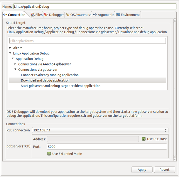
- Name the newly created debugger configuration, “LinuxApplicationDebug”, by editing its name in the Connection tab.
- In the Connection tab:
- For the Free Web Edition license, select Generic > gdb server > Linux Application Debug > Download and Debug Application.
- For the Subscription Edition or 30-day Evaluation Edition, select Linux Application Debug > Connections via gdbserver > Download and Debug Application.
- In the Connection tab, select the newly created RSE connection and keep the default values. Note: On some systems, you may need to uncheck the Use Extended Mode checkbox to prevent an ‘Unable to connect’ error.
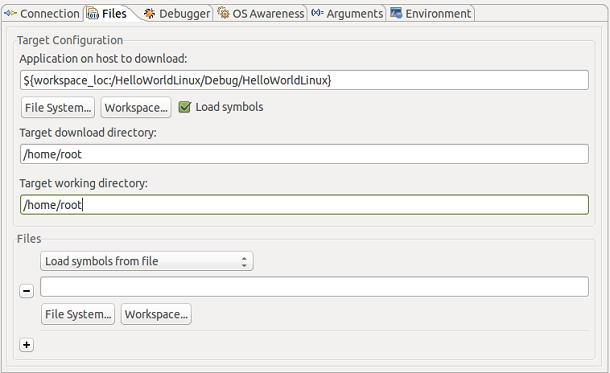
- Go to Files tab, and set the Target Configuration parameters:
- Select the Application on host to download to be the hello executable file. Use the Workspace… browse button.
- Edit the Target download directory to be "/home/root" (the root folder).
- Edit the Target working directory to be "/home/root" (the root folder).
- Click the Debug button. A dialog window appears asking to switch to Debug perspective. Click Yes.
- Eclipse downloads the application to the board and stops at main function entry.
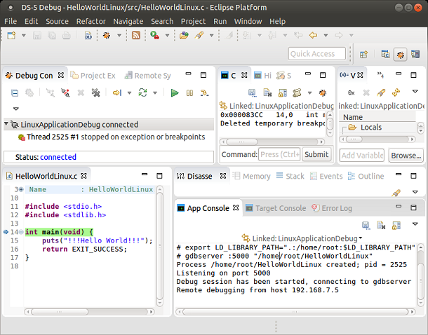
At this stage, all the usual debugging features of DS-5 can be used, such as breakpoints, view variables, registers, tracing, and threads.
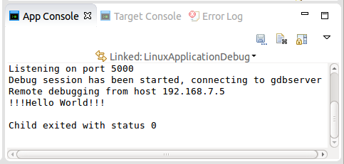
- Click the Continue green button or press F8 to run the application. The hello message is printed on the Application Console.
My First FPGA
Welcome to the My First FPGA tutorial. Here, we show you how to program your first FPGA device.
Click on the link below to check out the full tutorial where you learn to create the hardware equivalent of “Hello World”: a blinking LED. This is a simple exercise to get you started using the Intel® Quartus® software for FPGA development.
This tutorial shows you how to:
- Create a Quartus project
- Compile Verilog code
- Make pin assignments
- Program the FPGA to blink one of the eight green user LEDs on the board
We use a 50 MHz clock input (there’s an oscillator on board that drives the counter in the FPGA) to create a counter and assign an on-board LED to the nth bit of the counter.
Check out the full tutorial
Terasic DE10-Nano Diagrams and Schematics
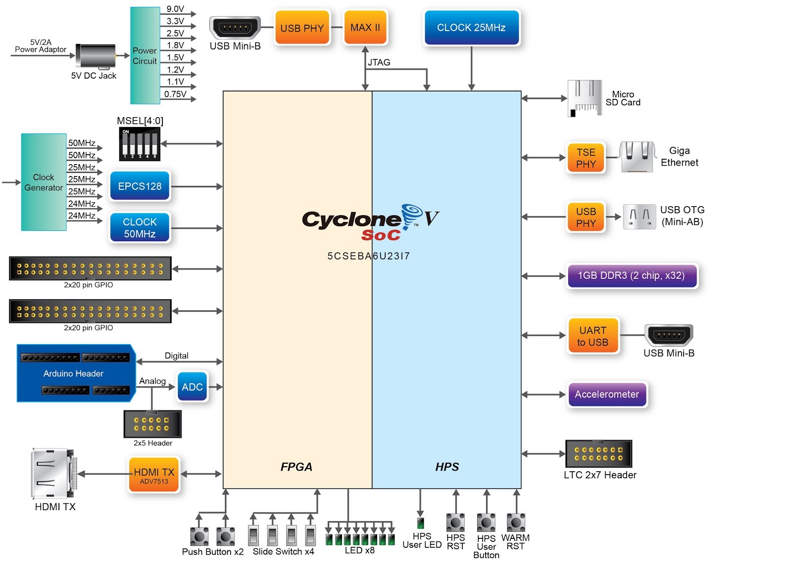
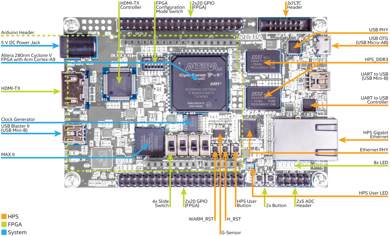
This section contains diagrams, schematics, and top and bottom level views of the Terasic DE10-Nano to help you learn more about the hardware and system-level design of the board.
Block Diagrams
Board Block Diagram
This is the board's high-level block diagram.
Board Schematic
Download the schematic for the DE10-Nano board.
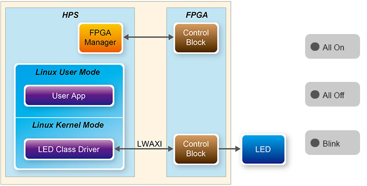
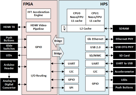
System Block Diagram
The system block diagram shows features enabled by the reference design that boots when the board is powered up. Blocks within the Hard Processor System (HPS) represent silicon features which do not change, whereas blocks within the FPGA are stored on the SD card and are loaded by the processor in the HPS after it boots.
Top and Bottom Views
Top View
Bottom View
For more complete information about compiler optimizations, see our Optimization Notice.
Terasic DE10-Nano Specifications
Hard Processor System
Processor
- Dual-core ARM* Cortex*-A9 MPCore processor at 800 MHz
- neon™ framework media-processing engine with double-precision floating point unit
- 32KB L1 instruction cache
- 32KB L1 data cache
- 512KB shared L2 cache
Memory
- 64KB on-chip SRAM
- 1GB DDR3 SDRAM (32-bit data)
- 8 GB microSD* flash memory card
Processor I/O
- 1 gigabit ethernet PHY with RJ45 connector
- 1 USB 2.0 OTG port, USB Micro-AB connector
- microSD* card interface and socket
- Accelerometer (I2C interface plus interrupt)
- UART to USB, USB Mini-B connector
- Warm reset button, cold reset button
- One user push button and one user LED
- Expansion header for use with Linear Technology* DC934A dual 16-bit digital-to-analog converter daughter card
Embedded software
- Linux* kernel 4.1.33 LTSI
- Angstrom* 2016.12
FGPA
Programmable Logic
- Logic elements (LE): 110KLE
- 5,570 kilobits memory
- 224 18 x 19 multipliers
- 112 variable precision DSP blocks
- 6 phased-locked loops (PLL)
- 145 User defined I/O
FPGA Configuration sources
- Embedded USB-Blaster* II (JTAG) cable
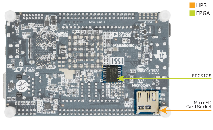
- Serial configuration flash - EPCS128
- ARM* Cortex*-A9 hard processor system (HPS)
FPGA I/O interfaces
- 2 push buttons
- 4 slide switches
- 8 LEDs
- Three 50 MHz clock sources from the clock generator
- Two 40-pin expansion headers with diode protection
- One Arduino* expansion header (Arduino UNO* R3 compatibility), can connect with Arduino shields
- One 10-pin analog input expansion header (shared with Arduino analog input)
- 8-channel, 12-bit A/D converter, 500 ksps, 4-pin serial peripheral interface (SPI)
Hardware Design
- 32-bit Fast Fourier Transform (FFT) engine
- HDMI* output (video pipeline)
- General-purpose I/O (GPIO) for LEDs, push buttons, and slide switches
- SPI primary interface to A/D converter
- I/F to Arduino shield headers (digital I/O, serial I/O, A/D converter)
Terasic DE10-Nano Appendix
This appendix contains additional resources to:
- Write an Image to the microSD* Card
- Extend the rootfs Partition
- How to Use Open PacKaGe management (OPKG)
- Build and Install the MRAA and UPM libraries
Write an Image to the MicroSD Card
This tutorial explains how to write an image to the microSD* card (removable flash memory) on the Terasic DE10-Nano. In the steps below, you'll learn where to download the latest image, how to write the image to the microSD card and what to look for (after powering on the board) to ensure you've correctly programmed the card.
Prerequisites:
- A Disk Imager
- A microSD to SD card adapter (optional)
Where to Get the Latest SD Card Image
The latest image can be downloaded from the Terasic DE10-Nano page.
Contents of the SD Card
The microSD card contains the embedded software needed to boot and run the board. These include the FPGA configuration bitstreams, Linux* kernel and device trees for the board, Angstrom* and U-Boot*.
Curious about the details of SD card contents? Find more information at the end of this tutorial page.
Download and Install the Image
Download the Image
- Get the desired image from the Terasic DE10-Nano page.
- Unpack tarball file (filename with file extension .tgz) using WinZip*.
Note Remember where you saved this file; you'll need it for step 6.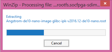
- For Windows* users, download Win32 Disk Imager*.
For Linux* users, learn How to write a disk image on Linux. - To program the microSD card from your host PC, insert the microSD card into the host PC. If a microSD card slot is not available, use a microSD to SD memory card adapter and then insert into a standard SD card slot.
- Open file explorer and check for the microSD card.
Note The microSD card is recognized as a mass storage device.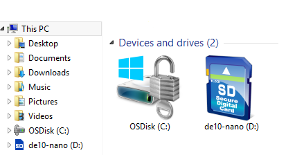
Write the image to the microSD* card
- Open Win32 Disk Imager
- Image File: Select image file
- Device: Point at target device (see step 5. above)
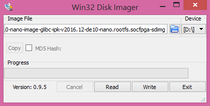
- Click Write to write image to the device (microSD card).
- Click OK and then hit Exit when write is successful.
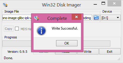
- Remove microSD card from host PC and insert into microSD card slot on the board.
LED Indicators
Power on the Board
To power on the board:
- Connect the USB OTG cable to the DE10-Nano (Micro-B) and your host PC (Type-A).
- Then connect the power adapter and plug in the power cable (DC 5V) into a wall outlet.
Note The board does not have a power button, and powering on the board here means connecting the power plug to a wall outlet.
LED Boot Sequence
- Blue LED: 3.3 V power LED lights up.
- Amber LED: Indicates that the FPGA has been configured.
- Green “Heartbeat” LED: A pulsing or heartbeat LED indicates that the Linux OS has been loaded.
- Green user LEDs [7:0]: Counts down from LSB to MSB. Indicates that the device tree overlay has been loaded. What that means is that Linux now knows about the LEDs (so why not blink them.).
If you've made it this far, it means everything is working. You're now ready to connect to the board and start playing with the web demos.
Extra: Details of SD Card Contents by Partition
In case you're interested, below are the contents of the SD card (factory default). Other SD card images contain other contents and could be partioned in other ways.
Partition 1
- FPGA configuration bitstreams
- Linux* kernel and device trees for the board
- extlinux.conf used for boot configuration by U-Boot
Partition 2
- Angstrom* RootFS
- Arm toolchain
- XFCE Desktop
- Examples/demos
Partition 3
- U-Boot SPL* and U-Boot*
Open PacKaGe management (OPKG)
Here, you'll find instructions for using Open PacKaGe Manager (OPKG), a lightweight package manager intended for embedded devices, to expand your development environment.
One of the benefits of having the board connected to the Internet is access to the Angstrom* package repositories. Over 1500 software libraries and tools are available and can be easily installed on the Terasic DE10-Nano board with the included package manager.
Default opkg configuration files are located under /etc/opkg/. You can specify which repository feeds to use by editing these files.
To update the list of available packages run:
opkg update
This command needs to be run again every time you make changes to the configuration file (e.g. adding a new repository).
You can learn more about OPKG.
Extend the rootfs Partition
Find below instructions for extending the microSD* (μSD) card root file system (rootfs) partition.
If the image has been deployed on a larger μSD card than the one included with the kit, the rootfs partition can be extended in order to claim the extra free space. This is an optional step and only recommended if you plan to install several additional software on the board, collect big data, or build libraries and tools from source. Please keep in mind that the following instructions use fdisk, a powerful, low-level partitioning tool that may render the image unusable if done incorrectly. In case something goes wrong, you will lose all the data on the μSD card will and have to rewrite the OS image.
For this we need the e2fsprogs-resize2fs tool, which can do a live resize a mounted partition live. It can be installed via opkg:
opkg install e2fsprogs-resize2fs
Then, run fdisk in interactive mode, and follow the steps shown. In short, we will list the existing partitions and take note of the start cylinder for the primary Linux* partition (rootfs). After this, delete the partition and create it again, using the exact same starting cylinder (this is very important).
For the end cylinder use the maximum value provided by your μSD card. This is generally the default value too. List the partitions again to check the changes and then write them. The warning received at the end is normal, since the file system is mounted and in use.
sh
root@de10-nano:~# fdisk /dev/mmcblk0

The number of cylinders for this disk is set to 236352.
There is nothing wrong with that, but this is larger than 1024,
and could in certain setups cause problems with:
1) software that runs at boot time (e.g., old versions of LILO)
2) booting and partitioning software from other OSs
   (e.g., DOS FDISK, OS/2 FDISK)

Command (m for help): p

Disk /dev/mmcblk0: 15.4 GB, 15489564672 bytes
4 heads, 32 sectors/track, 236352 cylinders
Units = cylinders of 128 * 512 = 65536 bytes

        Device Boot      Start         End      Blocks  Id System
/dev/mmcblk0p1   *          49        1648      102400   c Win95 FAT32 (LBA)
/dev/mmcblk0p2            1649       33648     2048000  83 Linux
/dev/mmcblk0p3              17          48        2048  a2 Unknown

Partition table entries are not in disk order

Command (m for help): d
Partition number (1-4): 2

Command (m for help): n
Command action
   e   extended
   p   primary partition (1-4)
p
Partition number (1-4): 2
First cylinder (1-236352, default 1): 1649
Last cylinder or +size or +sizeM or +sizeK (1649-236352, default 236352): Using default value 236352

Command (m for help): p

Disk /dev/mmcblk0: 15.4 GB, 15489564672 bytes
4 heads, 32 sectors/track, 236352 cylinders
Units = cylinders of 128 * 512 = 65536 bytes

        Device Boot      Start         End      Blocks  Id System
/dev/mmcblk0p1   *          49        1648      102400   c Win95 FAT32 (LBA)
/dev/mmcblk0p2            1649      236352    15021056  83 Linux
/dev/mmcblk0p3              17          48        2048  a2 Unknown

Partition table entries are not in disk order

Command (m for help): w
The partition table has been altered.
Calling ioctl() to re-read partition table
fdisk: WARNING: rereading partition table failed, kernel still uses old table: Device or resource busy
Finally, run resize2fs to extend the partition that was modified:
resize2fs /dev/mmcblk0p2
Build and Install the MRAA and UPM libraries
The MRAA and UPM libraries are bundled with the Terasic DE10-Nano image, which gets updated biannually. In some cases however, you might want to use the development branch to get access to the latest fixes and sensor drivers early. To achieve this, you'll have to build the MRAA and UPM libraries from source.
Prerequisites for a full MRAA and UPM install (C/C++, Java*, Node.js*, Python* 2.7, Python* 3):
opkg install cmake cmake-modules swig python-dev python3-dev nodejs nodejs-dev
For Java bindings, it should be possible to install openjdk-8 from an older Angstrom* repository. This can be done with opkg, simply download (42MB) and add the base feed to one of the opkg repository configuration files. To enable Java during a MRAA or UPM build, you will also have to pass the following flag to cmake `BUILDSWIGJAVA=ON`.
Additional build flags and complete build instructions for the MRAA library and for UPM. If you are having problems building the libraries from source, please open an issue with the corresponding library on GitHub*.