Visible to Intel only — GUID: GUID-82B5929D-948F-4581-9C63-15BA70F8C707
Refactor the Loop-Carried Data Dependency
Relax Loop-Carried Dependency
Transfer Loop-Carried Dependency to Local Memory
Minimize the Memory Dependencies for Loop Pipelining
Unroll Loops
Fuse Loops to Reduce Overhead and Improve Performance
Optimize Loops With Loop Speculation
Remove Loop Bottlenecks
Shannonization to Improve FMAX/II
Optimize Inner Loop Throughput
Improve Loop Performance by Caching On-Chip Memory
Global Memory Bandwidth Use Calculation
Manual Partition of Global Memory
Partitioning Buffers Across Different Memory Types (Heterogeneous Memory)
Partitioning Buffers Across Memory Channels of the Same Memory Type
Ignoring Dependencies Between Accessor Arguments
Contiguous Memory Accesses
Static Memory Coalescing
Conversion Rules for <span class='codeph'>ap_float</span>
Operations with Explicit Precision Controls
Comparison Operators
Additional <span class='codeph'>ap_float</span> Functions
Additional Data Types Provided by the <span class='codeph'>ap_float.hpp</span> Header File
Quality of Results and the ap_float Data Type
Specify Schedule FMAX Target for Kernels (<span class='codeph'>-Xsclock=<clock target>)
Disable Burst-Interleaving of Global Memory (<span class='codeph'>-Xsno-interleaving=<global_memory_type></span>)
Force Ring Interconnect for Global Memory (<span class='codeph'>-Xsglobal-ring</span>)
Force a Single Store Ring to Reduce Area (<span class='codeph'>-Xsforce-single-store-ring</span>)
Force Fewer Read Data Reorder Units to Reduce Area (<span class='codeph'>-Xsnum-reorder</span>)
Disable Hardware Kernel Invocation Queue (<span class='codeph'>-Xsno-hardware-kernel-invocation-queue</span>)
Modify the Handshaking Protocol Between Clusters (<span class='codeph'>-Xshyper-optimized-handshaking</span>)
Disable Automatic Fusion of Loops (<span class='codeph'>-Xsdisable-auto-loop-fusion</span>)
Fuse Adjacent Loops With Unequal Trip Counts (<span class='codeph'>-Xsenable-unequal-tc-fusion</span>)
Pipeline Loops in Non-task Kernels (<span class='codeph'>-Xsauto-pipeline</span>)
Control Semantics of Floating-Point Operations (<span class='codeph'>-fp-model=<var><value></var> </span>)
Modify the Rounding Mode of Floating-point Operations (<span class='codeph'>-Xsrounding=<rounding_type></span>)
Global Control of Exit FIFO Latency of Stall-free Clusters (<span class='codeph'>-Xssfc-exit-fifo-type=<var><value></var> </span>)
Enable the Read-Only Cache for Read-Only Accessors (<span class='codeph'>-Xsread-only-cache-size=<var><N></var>)</span>
Control Hardware Implementation of the Supported Data Types and Math Operations (<span class='codeph'>-Xsdsp-mode=<var><option></var> </span>)
Specify Schedule FMAX Target for Kernels
Specify a Workgroup Size
Specify Number of SIMD WorkItems
Omit Hardware that Generates and Dispatches Kernel IDs
Omit Hardware to Support the <span class='codeph'>no_global_work_offset</span> Attribute in <span class='codeph'>parallel_for</span> Kernels
Reduce Kernel Area and Latency
<span class='codeph'>disable_loop_pipelining</span> Attribute
<span class='codeph'>initiation_interval</span> Attribute
<span class='codeph'>ivdep</span> Attribute
<span class='codeph'>loop_coalesce</span> Attribute
<span class='codeph'>max_concurrency</span> Attribute
<span class='codeph'>max_interleaving</span> Attribute
<span class='codeph'>speculated_iterations</span> Attribute
<span class='codeph'>unroll</span> Pragma
Loop Fuse Functions and <span class='codeph'>nofusion</span> Attribute
Algorithmic C Data Types
Floating Point Pragmas
FPGA Accessor Properties
FPGA Extensions
FPGA Kernel Attributes
FPGA Local Memory Function
Latency Control Properties (Beta)
FPGA LSU Controls
FPGA Loop Directives
FPGA Memory Attributes
FPGA Optimization Flags
Pipe API
<span class='codeph'>task_sequence</span> Template Parameters and Function APIs
Visible to Intel only — GUID: GUID-82B5929D-948F-4581-9C63-15BA70F8C707
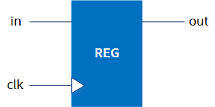
Register
A register is the most basic storage element in an FPGA. It has an input (in), an output (out), and a clock signal (clk). It is synchronous, that is, it synchronizes output changes to a clock. In an ALM, a register may store the output of the LUT.
The following figure illustrates a register:
Register
NOTE:
The clock signal is implied and not shown in some figures.
The following figure illustrates the waveform of register signals:
Waveform of Register Signals
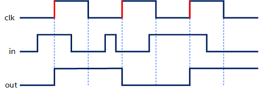
The input data propagates to the output on every clock cycle. The output remains unchanged between clock cycles.
Parent topic: FPGA Architecture Overview