Visible to Intel only — GUID: GUID-AEB66B70-9013-4133-A3B2-C08CECA9F1A8
Refactor the Loop-Carried Data Dependency
Relax Loop-Carried Dependency
Transfer Loop-Carried Dependency to Local Memory
Minimize the Memory Dependencies for Loop Pipelining
Unroll Loops
Fuse Loops to Reduce Overhead and Improve Performance
Optimize Loops With Loop Speculation
Remove Loop Bottlenecks
Shannonization to Improve FMAX/II
Optimize Inner Loop Throughput
Improve Loop Performance by Caching On-Chip Memory
Global Memory Bandwidth Use Calculation
Manual Partition of Global Memory
Partitioning Buffers Across Different Memory Types (Heterogeneous Memory)
Partitioning Buffers Across Memory Channels of the Same Memory Type
Ignoring Dependencies Between Accessor Arguments
Contiguous Memory Accesses
Static Memory Coalescing
Conversion Rules for <span class='codeph'>ap_float</span>
Operations with Explicit Precision Controls
Comparison Operators
Additional <span class='codeph'>ap_float</span> Functions
Additional Data Types Provided by the <span class='codeph'>ap_float.hpp</span> Header File
Quality of Results and the ap_float Data Type
Specify Schedule FMAX Target for Kernels (<span class='codeph'>-Xsclock=<clock target>)
Disable Burst-Interleaving of Global Memory (<span class='codeph'>-Xsno-interleaving=<global_memory_type></span>)
Force Ring Interconnect for Global Memory (<span class='codeph'>-Xsglobal-ring</span>)
Force a Single Store Ring to Reduce Area (<span class='codeph'>-Xsforce-single-store-ring</span>)
Force Fewer Read Data Reorder Units to Reduce Area (<span class='codeph'>-Xsnum-reorder</span>)
Disable Hardware Kernel Invocation Queue (<span class='codeph'>-Xsno-hardware-kernel-invocation-queue</span>)
Modify the Handshaking Protocol Between Clusters (<span class='codeph'>-Xshyper-optimized-handshaking</span>)
Disable Automatic Fusion of Loops (<span class='codeph'>-Xsdisable-auto-loop-fusion</span>)
Fuse Adjacent Loops With Unequal Trip Counts (<span class='codeph'>-Xsenable-unequal-tc-fusion</span>)
Pipeline Loops in Non-task Kernels (<span class='codeph'>-Xsauto-pipeline</span>)
Control Semantics of Floating-Point Operations (<span class='codeph'>-fp-model=<var><value></var> </span>)
Modify the Rounding Mode of Floating-point Operations (<span class='codeph'>-Xsrounding=<rounding_type></span>)
Global Control of Exit FIFO Latency of Stall-free Clusters (<span class='codeph'>-Xssfc-exit-fifo-type=<var><value></var> </span>)
Enable the Read-Only Cache for Read-Only Accessors (<span class='codeph'>-Xsread-only-cache-size=<var><N></var>)</span>
Control Hardware Implementation of the Supported Data Types and Math Operations (<span class='codeph'>-Xsdsp-mode=<var><option></var> </span>)
Specify Schedule FMAX Target for Kernels
Specify a Workgroup Size
Specify Number of SIMD WorkItems
Omit Hardware that Generates and Dispatches Kernel IDs
Omit Hardware to Support the <span class='codeph'>no_global_work_offset</span> Attribute in <span class='codeph'>parallel_for</span> Kernels
Reduce Kernel Area and Latency
<span class='codeph'>disable_loop_pipelining</span> Attribute
<span class='codeph'>initiation_interval</span> Attribute
<span class='codeph'>ivdep</span> Attribute
<span class='codeph'>loop_coalesce</span> Attribute
<span class='codeph'>max_concurrency</span> Attribute
<span class='codeph'>max_interleaving</span> Attribute
<span class='codeph'>speculated_iterations</span> Attribute
<span class='codeph'>unroll</span> Pragma
Loop Fuse Functions and <span class='codeph'>nofusion</span> Attribute
Algorithmic C Data Types
Floating Point Pragmas
FPGA Accessor Properties
FPGA Extensions
FPGA Kernel Attributes
FPGA Local Memory Function
Latency Control Properties (Beta)
FPGA LSU Controls
FPGA Loop Directives
FPGA Memory Attributes
FPGA Optimization Flags
Pipe API
<span class='codeph'>task_sequence</span> Template Parameters and Function APIs
Visible to Intel only — GUID: GUID-AEB66B70-9013-4133-A3B2-C08CECA9F1A8
Kernel Memory Viewer
Data movement is a bottleneck in many algorithms. The Kernel Memory Viewer shows you how the Intel® oneAPI DPC++/C++ Compiler interprets the data connections and synthesizes memory for your kernel. Use the Kernel Memory Viewer to help identify data movement bottlenecks in your kernel design.
Some patterns in memory accesses can cause undesired arbitration in the load-store units (LSUs), affecting the throughput performance of your kernel. Use the Kernel Memory Viewer to identify unwanted arbitration in the LSUs.
To analyze your SYCL* system, click Views > Kernel Memory Viewer.
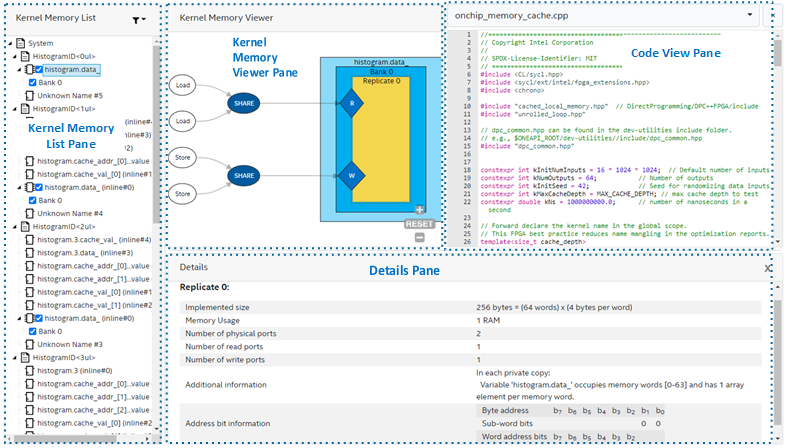
The following image illustrates the layout of the Kernel Memory Viewer:
Kernel Memory Viewer Layout
The Kernel Memory Viewer has the following panes:
Pane |
Description |
|---|---|
Kernel Memory List |
Lists all memories present in your design. When you select a memory name, you can view its graphical representation in the Kernel Memory Viewer pane. |
Kernel Memory Viewer |
Shows a graphical representation of the memory system or memory bank selected in the Kernel Memory List pane. |
Code View |
Shows the source code file for which the reports are generated. |
Details |
Shows the details of the memory system or memory bank selected in the Kernel Memory List pane. |
Kernel Memory List
The Kernel Memory List pane displays a kernel hierarchy with memories synthesized (RAMs, ROMs, and registers) and optimized away in that kernel.
Features and Details of the Kernel Memory List Pane

The following table describes each numbered feature highlighted in the above image:
No. |
Icon or Label |
Name |
Description |
|---|---|---|---|
1 |
Kernel name |
You can expand or collapse the list of memories in your kernel. Memories that do not belong to any kernel are displayed under (Other). |
|
2 |
RAM |
A RAM is a memory that has at least one write to it. The name of the RAM memory is the same as its name in your design. When you select a memory name, you can view a logical representation of the RAM in the Kernel Memory Viewer pane. By default, only the first bank of the memory system is displayed. To select banks that you want the Kernel Memory Viewer pane to display:
|
|
3 |
ROM |
A ROM is a read-only memory. The name of the ROM memory is same as its name in your design. When you select a memory name, you can view a logical representation of the ROM in the Kernel Memory Viewer pane. By default, only the first bank of the memory system is displayed. To select banks that you want the Kernel Memory Viewer pane to display:
|
|
4 |
Bank #num |
Bank |
A memory bank is always associated with a RAM or a ROM. Each bank is named Bank #num, where #num is the memory bank's ID starting from 0.
|
5 |
Register |
A register is a kernel variable carried through the pipeline in registers (rather than being stored in a RAM or ROM). The name of the register is the same as its name in your design. A register variable is implemented either exclusively in FFs or in a combination of FFs and RAM-based FIFOs. |
|
6 |
Text label |
Optimized Away |
A kernel variable can be optimized away because it is unused in your design, or compiler optimizations have transformed all uses of the variable such that it is unnecessary. The name of the optimized away variable is the same as its name in your design. |
7 |
Filter |
Use the Kernel Memory List filter to selectively view the list of RAMs, ROMs, registers, and optimized away variables in your design. When you clear the checkbox associated with an item in the filter, you hide all occurrences of that kind of item in the Kernel Memory List. Filter your Memory List to help you focus on a specific type of memory in your design. |
Kernel Memory Viewer
In the Kernel Memory Viewer pane, you can view connections between loads and stores to specific logical ports on the banks in a memory system. You can also view the number of replicates and private copies created per bank for your memory system. You can see the following types of nodes in the Kernel Memory Viewer pane, depending on the kernel memory system and your selection in the Kernel Memory List pane:
Node Type |
Description |
|---|---|
Memory node |
The memory system for a given variable in your design. |
Bank node |
A bank in the memory system. A memory system contains at least one bank. A memory bank can connect to one or more port nodes. |
Replication node |
A replication node shows memory bank replicates created to support multiple accesses to a local memory efficiently. A bank contains at least one replicate. You can view replicate nodes when you view a memory bank by clicking its name in the Kernel Memory List pane. |
Private-copy node |
A private-copy node shows private copies within a replicate created to allow simultaneous execution of multiple loop iterations. A replicate contains at least one private copy. You can view private-copy nodes when you view a memory bank by clicking its name in the Kernel Memory List pane. |
Port node |
Each read or write access to local memory is mapped to a port. The logical port for a bank. There are three types of ports:
|
LSU node |
A store (ST) or load (LD) node connected to the memory through port nodes. |
Arbitration node |
An arbitration (ARB) node shows that LSUs compete for access to a shared port node, which can lead to stalls. |
Port-sharing node |
A port-sharing node (SHARE) shows that LSUs have mutually exclusive access to a shared port node, so the load-store units are free from stalls. |
Within the graphical representation of a memory in the Kernel Memory Viewer pane, you can perform the following:
- Hover over any node to view the attributes of that node.
- Hover over an LSU node to highlight the path from the LSU node to all ports to which the LSU connects.
- Hover over a port node to highlight the path from the port node to all LSUs that read or write to the port node.
- Click a node to select it and display the node attributes in the Details pane.
The following images illustrate examples of what you see in the Kernel Memory Viewer:
Logical Representation of a Memory in the Kernel Memory Viewer Pane

Bank View of a Memory Bank in the Kernel Memory Viewer Pane

Code View
The Code View pane displays your source code. When you click on a memory or a bank in the Kernel Memory Viewer pane, the code view pane highlights the line of your code where you declared the memory.
Details
The Details pane shows the attributes of the node selected in the Kernel Memory Viewer pane. For example, when you select a memory in a kernel, the Details pane displays the following information:
- Width and depths of memory banks
- Memory layout
- Address-bit mapping
- Memory attributes that you specified in your source code
The content of the Details pane persists until you select a different node in the Kernel Memory Viewer pane.
Parent topic: Review the FPGA Optimization Report